

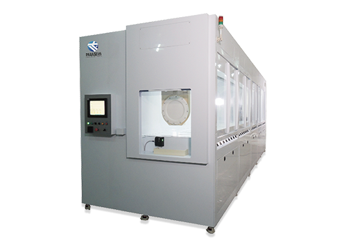
Semi-Automatic TSV Plating Equipment
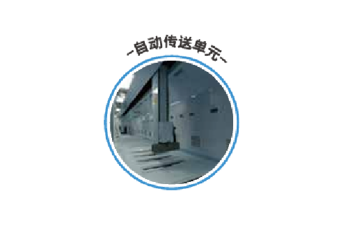
The Semi-Automatic TSV Plating Equipment is a core process tool specifically designed for Through-Silicon Via technology development and small-to-medium volume production. It utilizes a precision electrochemical deposition system to fill millions of micron-scale deep holes on wafers with high-purity metals (such as copper), enabling vertical electrical interconnections in 3D chip stacking. Operating in a "semi-automatic" mode, the equipment requires manual wafer loading/unloading and initial alignment, while subsequent critical processes—including degassing, plating, cleaning, and drying—are fully automated. This ensures high uniformity, void-free filling, and excellent step coverage within the TSVs.
Application Fields & Scenarios
Core Application Fields:
Advanced Packaging: Widely used in manufacturing vertical interconnect structures for 2.5D/3D IC packaging, CIS (Image Sensor) packaging, fan-out packaging, and more.
Micro-Electro-Mechanical Systems (MEMS): Provides metallization solutions for deep holes and trenches in MEMS devices.
Typical Application Scenarios:
TSV Process R&D and Optimization: Suitable for R&D institutes, universities, and corporate process development lines, facilitating rapid parameter debugging and recipe validation.
Small-Batch Multi-Variety Production: Meets pilot production and scaled trial production needs for specialized devices such as CIS, high-end MEMS sensors, and AI chips.
Capacity Supplement & Flexible Manufacturing: Serves as a supplement to fully automated production lines, offering highly flexible plating solutions for special products and R&D projects.
The equipment achieves the optimal balance between performance and cost, serving as a vital platform to advance 3D integration technology from the laboratory to industrialization.
Related Products
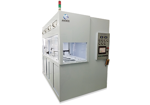
Aluminum Housing Nickel-Gold Plating Equipment
Applications: Aerospace & Military Electronics, High-End Communication Equipment, Precision Medical Devices
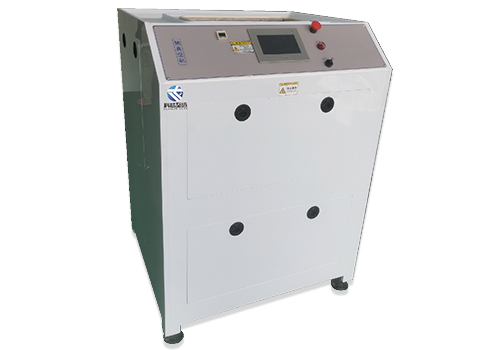
TSV Plating Pre-Vacuum Treatment
Applications: 2.5D/3D IC Packaging, High-End Image Sensors (CIS), Micro-Electro-Mechanical Systems (MEMS)
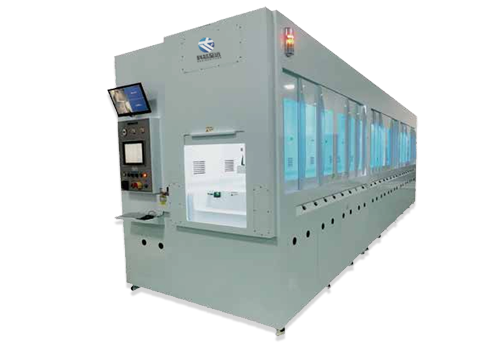
Semi-Automatic Wafer Plating Equipment
Integrated Circuit Manufacturing, Advanced Semiconductor Packaging, Micro-Electro-Mechanical Systems (MEMS), Compound Semiconductors, and Scientific Research