

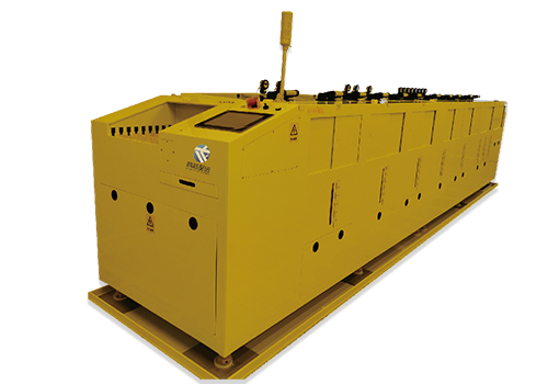
Horizontal Develop Machine
The Horizontal Develop Machine is a critical equipment in the semiconductor lithography process, specifically designed for photoresist patterning on wafers after exposure. It adopts a horizontal transfer architecture where wafers are placed flat and sequentially transferred between enclosed process chambers via robotic arms.
Its standard process flow includes: precise spray development to dissolve the photoresist in exposed (or unexposed) areas, followed by deionized water spin rinse to rapidly terminate the reaction and remove residues, and finally high-speed spin drying. This horizontal design effectively reduces chemical residue and liquid disturbance, ensuring high uniformity, high resolution, and low defect rates in the development process, making it a core guarantee for precise pattern transfer.
Application Fields
This equipment is essential for any field involving photolithographic patterning processes.
Core Application Fields:
Integrated Circuit Manufacturing: Used for photoresist development in front-end processes from micron to nanometer nodes.
Advanced Semiconductor Packaging: Completes patterning in wafer-level packaging, bump preparation, redistribution layer processes.
MEMS Manufacturing: Used for creating complex microstructure patterns on silicon wafers for MEMS devices.
Extended Application Scenarios:
Flat Panel Display: Manufacturing array substrates for TFT-LCD and OLED panels.
Optoelectronic Devices & LED: Used in manufacturing photonic chips, lasers, LED patterned substrates.
Magnetic Head Manufacturing and other precision micro-patterning fields.
The process stability of the horizontal develop machine directly determines the quality of lithographic patterns, making it a critical step affecting device performance and final product yield.
Related Products
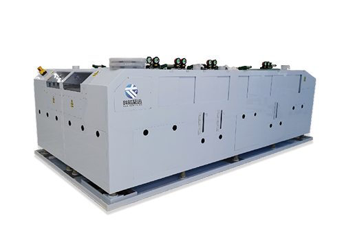
Rotary Copper-Titanium Etching Machine
Applications: Advanced Semiconductor Packaging, MEMS Device Fabrication, Medical Implants & Precision Instruments
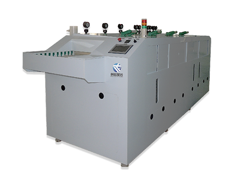
Horizontal Copper Etching Machine
Applications: Integrated Circuit Manufacturing, Packaging Substrates & HDI PCB, Flat Panel Display
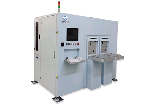
Inline Auto Loader/Unloader
Applications: Semiconductor & Electronics Manufacturing, Automotive & Components, Photovoltaic Industry